PCB Reverse Engineering, Redesign & Repair
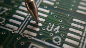
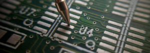
ScanCAD is the provider of the only system in the world that can take a physical circuit board and fully reverse engineer it to provide complete manufacturing CAD data and even native format schematics. The system includes the ability to capture precise form, fit and function for all layers of the PCB, including all inner layer geometries, drill, drill plating and layer thickness, cutouts, outline, silkscreen, and even blind or buried vias.
Data generated from PCB Reverse Engineering can be used either to manufacture replacement parts, or provide insight in repairing existing parts when schematics may not be available.
PCB Reverse Engineering Systems
Why do I need to reverse engineer a CCA/PCB?

One of the largest problems that a company can face over the lifetime of an electric device is the maintenance of circuit board assemblies (CCAs) as replacement parts. This is much less important for consumer grade products such as electronics in toys, but far more important for complex legacy control, communication, transportation, navigation and other electronic systems.
Components and boards can be damaged for many reasons including temperature, power fluctuation, mistreatment, aging and even insects/rodents. In many cases, failure of a single component can cause massive, complex systems to stop. Ultimately, when a component in a complex electrical system fails, you will need to merge replacement elements into the existing infrastracture. One way to do this is to design a new board based off of schematics and parts lists, but this process will not yield a board with the exact same characteristics which can lead to potential integration problems. Additionally, certain aplications have extremely rigorous and time consuming qualification processes before you can install your shiny new CCA. You may even have to go through several revisions of design and prototyping before you have a working solution.
Why go through a lengthy, complicated redesign and qualification process when you can copy and reproduce an identical board with identical functions?
ScanCADs PCB RE process is just that – taking an existing board, and generating design data to re-produce the exact same part that failed. The benefit of this process is that you do not have to endure a lengthy redesign and prototyping cycle since you will be matching the form, fit and function of the original part.
Reverse Engineering Systems
In order to generate circuit board data, ScanCADs PCB RE System utilizes proprietary milling techniques and high resolution, calibrated images as a base for generating gerber data. With a destructive RE process, each layer is imaged and aligned, and then using automated and manual processes, gerber data is generated for all layers of the circuit board. This process allows gerber data to be generated that matches the exact form, fit and function of the original board due to the fact that inner layer copper plane and circuit geometries are captured and digitized.

The resulting data can be validated against a golden, functional board and the netlist verified to ensure proper connections between components. Once all data is captured for the board, the project is moved to the schematic generation phase, where all of the acquired data is merged into schematic.
For boards that cannot be destroyed, ScanCADs PCB RE system also supports non- destructive reverse engineering processes. While the FPT process does not yield inner layer geometries, it still produces connectivity information and can be used in conjunction with BOM information to create a schematic without physically destroying the board.
Our Supplier for Reverse Engineering Systems: ScanCad

Your Contact