Inspection Systems
Since 1990, thousands of customers in 50+ countries have utilized ScanCAD’s powerful family of low cost, flat-bed scanner based tools. ScanCAD’s advanced scanning and software technologies have been used for process management, inspection and data creation in the electronics, photo chemical machining, semiconductor, aerospace, medical, energy, aluminum extrusion, automotive, construction, industrial, photovoltaic solar, fuel cell, electrical machinery, textile and military industries. ScanCAD International improves the quality of life for customers, employees and the world by providing high quality, innovative solutions that simplify complex technology in a positive, environmentally-conscious manner while having fun along the way!
Process Control
The apparently simple operation of placing components on a circuit board is far more delicate than it seems. This single operation actually requires a careful balance between manufacturing tolerances/accuracy of a variety of different systems. First, the solder paste stencil (usually sourced externally) is produced from a master dataset. Solder paste stencil fabrication is a fairly accurate process, however like anything, is subject to the real world, and thus manufacturing tolerances. The resultant stencil will inevitably vary from the master dataset. Second, a batch of boards is fabricated. PCB fabrication tends to be far less accurate and results in a job lot of circuit boards that are generally consistent internally, but are subject to significant deviation from the original design. The stencil and the board are brought together and paste is deposited on the board. Lastly, components are placed on the circuit board, again using coordinate locations supplied by the master dataset.
In theory everything comes together beautifully at this point and there are no errors!

In reality the additive differences from the stencil, the board, and the component placement machine overcome the tolerance of the process, and defects are introduced. Defects are generally seen on the smallest pitch devices where the tolerance is the tightest and they are generally randomly distributed. It can be a nightmare trying to track down and minimize or eliminate these defects because there is no single failure point. Component placement machine operators may spend hours simply adjusting offsets in order to get the boards to run. There must be a better way!
Address the Root Cause
The root cause is not a failure in any one of the elements coming together. More than likely, the stencil is manufactured within specification, the board is manufactured within specification, and the component placement machines are calibrated and operating within specification. The problem is the cumulative tolerance deviation that occurs when all three of these independent processes come together on the production line violating what is required for error-free placement. The window of alignment for all three elements could be too small to operate within.
Instead of fighting with offsets and trying to force an overtaxed system to operate – address the root cause!
The root cause is that the stencil, the board, and the component placement machine are all compounding tolerances together at the time of solder paste printing and component placement.
Defects at this stage are expensive, difficult to understand, and unnecessary.
Improve your Process
Instead of using the same master dataset for all three stages, follow a more modern approach. Use the master dataset in order to manufacture the job lot of circuit boards. Then, use our systems to modify the stencil and component data to match the job lot of PCB’s exactly. In effect, the tolerances are no longer compounded and errors in solder paste deposition and component placement are reduced dramatically. Furthermore, our process allows potential issues with either the stencil, or the board, to be detected upstream and before value is added and material wasted.
Reduce defects, save operator time, and increase yield.
Unique Technology
Internally developed software coupled with our low-cost vision platform and NIST certified calibration equipment ensures that our system is a solution that is custom tailored to help you improve your processes and give you the visibility and insight you need. Our proven hardware and software have been specifically designed to maintain an excellent price-performance ratio, maximize your ROI and provide a unique set of tools for effective and efficient process improvement.
100% traceability and SPC data for your quality certification and compliance requirements.
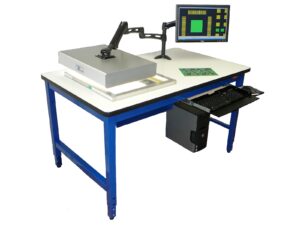
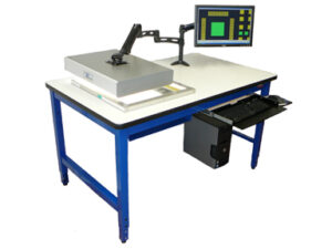
Inspection of Stencils and Screens
ScanCAD has been supporting solder paste stencil and emulsion screen fabricators and users for over 20 years. We are the global leader in flexible, multi-purpose screen and stencil inspection systems. Our system captures calibrated high resolution images, overlays original CAD or Golden Part data and performs an automatic inspection to detect errors BEFORE production. By eliminating errors prior to production, we are able to significantly decrease costly rework and scrap
The ScanCAD system can inspect all types of stencils, screens and even the precision phototools used to create emulsion screens. Whether you are inspecting an incoming stencil or screen to ensure conformity, confirming all apertures were properly cleaned in between runs, or performing a periodic check to ensure wear is within tolerance; our systems are a critical component of process control.
ScanCAD Inspection systems are a critical component for process control.
Unique Niche
Independent verification of stencils and screens is mandatory for ensuring no bad parts are used in production. Even one defective stencil or screen defect can be very costly due to scrap, rework or even product recall. These systems can also be used as general purpose measurement & inspection systems for parts such as bare PCB’s, pallets, carriers, tooling, ceramics/LTCC, solder paste, glue, etc.
Unique Technology
Internally developed software coupled with our low-cost vision platform and NIST certified calibration equipment ensures that our system is a solution that is custom tailored for your application. Our hardware and software have been specifically designed to maintain an excellent price-performance ratio, maximize your ROI and provide a unique set of tools for effective and efficient inspection & measurement providing 100% traceability and SPC data for your ISO certification.
Unique Process
Over our thirty years in business, we have continuously improved our process to support cutting edge technology. Our ability to inspect relative to both the fabrication data (eg. cut file for laser stencils) and the original design file (eg. PCB CAD file for stencils), as well as automatically compare directly against an actual part (eg. PCB) sets our system apart. In addition, the same system can also generate fabrication data that exactly matches the substrate (eg. Creating stencil data for an existing PCB) which has been proven to reduce production defects.
A 43% reduction in solder paste defects can be achieved by simply adjusting stencil data to match a job lot of PCBs. Why compound process errors if you don’t have to? It’s time to up-level your process.
Manufacturers of Inspection Systems: ScanCAD & Midas Vision Systems

Your Contact